
What Inspection Processes Are Used in Flex PCB Fabrication?
Flex PCB fabrication is a highly specialized process that requires careful attention to detail to ensure the final product meets the strict standards required for various applications, such as medical devices, wearable electronics, and automotive systems. Given the unique properties of flexible printed circuit boards (PCBs), such as their ability to bend, twist, and conform to specific shapes, manufacturers use a range of inspection processes to guarantee the integrity and functionality of the circuits. These inspection processes are essential for detecting defects, verifying quality, and ensuring the reliability of the flex PCB in its intended application.
Visual Inspection for Surface Defects
One of the first steps in the inspection process during flex PCB fabrication is visual inspection. This involves checking the surface of the PCB for any visible defects, such as scratches, dents, or imperfections in the solder mask and copper traces. Visual inspection can be performed manually or with the aid of automated optical inspection (AOI) systems. AOI systems use high-resolution cameras and image processing software to detect surface defects that might be difficult to see with the naked eye.
In addition to identifying defects in the copper traces and solder mask, visual inspection also ensures that components are correctly placed on the flex PCB and that there are no misalignments. This step is critical to ensure that the PCB meets the required specifications and that all parts are correctly positioned for optimal performance.
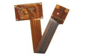
Automated Optical Inspection (AOI) for Precision Checking
Automated Optical Inspection (AOI) is an advanced inspection process widely used in flex pcb fabrication. AOI systems capture high-resolution images of the PCB surface and compare them to predefined design data to identify any discrepancies. The system can detect issues such as shorts, open circuits, misalignment, and incorrect component placement. This method provides a high level of accuracy and is especially useful in detecting subtle defects that may not be visible during manual inspection.
In flex PCB fabrication, AOI is particularly beneficial for inspecting the fine lines and narrow traces typically used in flexible circuits. The flexibility and thinness of these PCBs make them prone to defects such as copper trace breakage or misalignment during the assembly process. AOI ensures that these issues are detected early, preventing potential failures in the final product.
X-Ray Inspection for Inner Layer Defects
In multi-layer flex PCBs, which are commonly used in applications requiring high-density circuits, X-ray inspection is a valuable tool for detecting defects in the inner layers of the board. This non-destructive method allows manufacturers to inspect internal structures, such as vias, pads, and interlayer connections, that are otherwise inaccessible through visual inspection.
X-ray inspection helps identify issues such as voids in solder joints, misaligned vias, and incomplete connections between layers. It is particularly important for flex PCB fabrication, as these boards often have multiple layers stacked together, making internal inspections crucial for ensuring the reliability and performance of the final product.
Electrical Testing for Functionality Verification
Electrical testing is a critical inspection process in flex PCB fabrication. This method involves applying electrical signals to the PCB and measuring the responses to verify that the circuit functions correctly. One of the most common types of electrical testing is the in-circuit test (ICT), which checks the electrical paths of the PCB for continuity, resistance, and correct component placement.
For flex PCBs, electrical testing is essential to ensure that all signals pass through the circuit as intended and that there are no open or short circuits. This testing helps identify potential faults that could compromise the functionality of the device in real-world applications, such as signal loss or data transmission errors.
Microsectioning for Detailed Analysis
Microsectioning is a more advanced inspection process used in flex PCB fabrication to analyze the internal layers of the PCB in detail. In this process, a small cross-section of the PCB is cut and then polished to examine the layers, via plating, and the quality of the material bonding. This method helps detect issues such as poor adhesion between layers, insufficient via plating, or internal damage that might not be visible through surface inspection.
Microsectioning provides valuable information for assessing the overall quality of the PCB and ensuring that all layers are properly constructed and bonded. This process is particularly useful in high-reliability applications, such as medical or aerospace devices, where the integrity of each layer is crucial for the device’s performance.
Final Inspection and Functional Testing
Once all individual inspections are complete, a final inspection is performed to ensure the overall quality of the flex PCB. This includes checking the final dimensions, verifying component placements, and ensuring that all design specifications are met. In addition to visual and electrical inspections, functional testing is often carried out to simulate real-world operating conditions and verify that the PCB performs as expected in its intended application.
Conclusion
Inspection processes play a vital role in flex PCB fabrication, ensuring that the final product meets the high standards required for various demanding applications. From visual and automated optical inspections to advanced X-ray and electrical testing, these processes help detect defects early, maintain high-quality standards, and ensure the reliability of flexible circuit boards. As technology continues to evolve, the inspection processes used in flex PCB fabrication will become even more sophisticated, enabling manufacturers to produce flexible, durable, and high-performance circuits for a wide range of industries.